- 您现在的位置:买卖IC网 > Sheet目录1214 > EVAL-ADG788EBZ (Analog Devices Inc)BOARD EVALUATION FOR ADG788
�� ��
��
��EVAL-ADG788EBZ�
�EVALUATION� BOARD� HARDWARE�
�The� ADG788� evaluation� board� kit� contains� the� following:�
�POWER� SUPPLY�
�?�
�?�
�A� fully� fitted� printed� circuit� board�
�A� CD� containing� the� ADG788� product� data� sheet� and� the�
�evaluation� board� data� sheet�
�To� operate� the� ADG788� evaluation� board,� the� user� must� provide�
�an� external� power� supply� connected� to� Power� Block� P1.� The�
�supply� voltage� range� is� 1.8� V� to� 5.5� V� for� single-supply� operation�
�and� ±2.5� V� for� dual-supply� operation.� The� user� can� select� single-�
�The� evaluation� board� allows� the� user� to� connect� the� signals� that�
�require� switching� to� the� ADG788� switch� and� control� its� operation�
�by� using� the� on-board� links� or� by� applying� the� correct� control�
�signals� to� the� appropriate� connectors.� The� signals� present� at� the�
�supply� operation� or� dual-supply� operation� using� Link� J23,� as� shown�
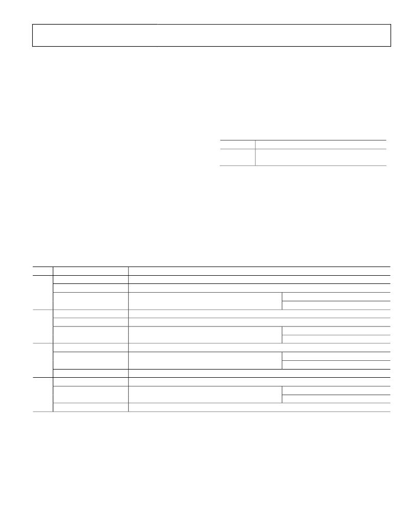
��Table� 1.� Link� J23� Configuration�
�pins� of� the� ADG788� can� be� monitored� using� the� test� point�
�provided� on� the� board.�
�The� following� sections� describe� the� function� of� all� connectors�
�Position�
�A�
�B�
�Operation� Mode�
�Single-supply� operation�
�Dual-supply� operation� (default� configuration)�
�and� links.�
�SWITCH� CONTROL�
�The� four� input� pins,� IN1,� IN2,� IN3,� and� IN4,� control� the� opera-�
�tion� of� the� ADG788.� Link� J8,� Link� J9,� Link� J12,� and� Link� J13�
�control� the� logic� levels� applied� to� these� pins� and� allow� the� user�
�to� drive� these� pins� with� external� signals� applied� to� Connector� J5�
�and� Connector� J11� (the� signals� have� 50� Ω� on-board� termination�
�resistors� to� GND).� Table� 2� describes� the� configuration� achieved�
�for� each� position� of� these� links.�
�Table 2. Link J8, Link J9, Link J12,� and� Link� J13� Settings�
�Link�
�J8�
�Position�
�Removed�
�A�
�ADG788� Switch� Status�
�S2A� to� D2� =� off,� S2B� to� D2� =� on�
�S2A� to� D2� =� on,� S2B� to� D2� =� off�
�B� (default� configuration)�
�Controlled� via� signal� applied� to� Connector� J5_TOP�
�High:� S2A� to� D2� =� on,� S2B� to� D2� =� off�
�Low:� S2A� to� D2� =� off,� S2B� to� D2� =� on�
�J9�
�Removed�
�A�
�S3A� to� D3� =� off,� S3B� to� D3� =� on�
�S3A� to� D3� =� on,� S3B� to� D3� =� off�
�B� (default� configuration)�
�Controlled� via� signal� applied� to� Connector� J5_BOTTOM�
�High:� S3A� to� D3� =� on,� S3B� to� D3� =� off�
�Low:� S3A� to� D3� =� off,� S3B� to� D3� =� on�
�J12�
�Removed�
�S1A� to� D1� =� off,� S1B� to� D1� =� on�
�A� (default� configuration)�
�B�
�Controlled� via� signal� applied� to� Connector� J11_BOTTOM�
�S1A� to� D1� =� on,� S1B� to� D1� =� off�
�High:� S1A� to� D1� =� on,� S1B� to� D1� =� off�
�Low:� S1A� to� D1� =� off,� S1B� to� D1� =� on�
�J13�
�Removed�
�S4A� to� D4� =� off,� S4B� to� D4� =� on�
�A� (default� configuration)�
�B�
�Controlled� via� signal� applied� to� Connector� J11_TOP�
�S4A� to� D4� =� on,� S4B� to� D4� =� off�
�Rev.� 0� |� Page� 3� of� 8�
�High:� S4A� to� D4� =� on,� S4B� to� D4� =� off�
�Low:� S4A� to� D4� =� off,� S4B� to� D4� =� on�
�发布紧急采购,3分钟左右您将得到回复。
相关PDF资料
EVAL-ADM1021AEB
BOARD EVAL FOR ADM1021
EVAL-ADM1023EB
BOARD EVAL FOR ADM1023
EVAL-ADM1031EB
BOARD EVAL FOR ADM1031
EVAL-ADM1062TQEBZ
BOARD EVALUATION FOR ADM1062TQ
EVAL-ADM1075CEBZ
BOARD EVAL FOR ADM1075
EVAL-ADM1087EBZ
BOARD EVALUATION FOR ADM1087
EVAL-ADM1166TQEBZ
BOARD EVAL FOR ADM1166TQ
EVAL-ADM1168LQEBZ
BOARD EVAL FOR ADM1168LQ
相关代理商/技术参数
EVAL-ADG790EBZ
功能描述:BOARD EVALUATION ADG790 RoHS:是 类别:编程器,开发系统 >> 评估演示板和套件 系列:- 标准包装:1 系列:- 主要目的:电信,线路接口单元(LIU) 嵌入式:- 已用 IC / 零件:IDT82V2081 主要属性:T1/J1/E1 LIU 次要属性:- 已供物品:板,电源,线缆,CD 其它名称:82EBV2081
EVAL-ADG791GEBZ
制造商:Analog Devices 功能描述:EVALUATION BOARD I.C. - Bulk
EVAL-ADG792GEBZ
制造商:Analog Devices 功能描述:EVALUATION BOARD I.C. - Bulk
EVAL-ADG793GEB2
制造商:AD 制造商全称:Analog Devices 功能描述:I2C-Compatible, Wide Bandwidth, Triple 3:1 Multiplexer
EVAL-ADG793GEBZ
制造商:Analog Devices 功能描述:Evaluation Boards For The ADG79XX Family Of Switches 制造商:Analog Devices 功能描述:EVALUATION BOARD I.C. - Bulk
EVAL-ADG795GEB2
制造商:AD 制造商全称:Analog Devices 功能描述:I2C-Compatible, Wide Bandwidth, Five 2:1 Multiplexer
EVAL-ADG795GEBZ
制造商:Analog Devices 功能描述:EVALUATION BOARD I.C. - Bulk
EVAL-ADG796AEB
制造商:AD 制造商全称:Analog Devices 功能描述:I2C-Compatible, Wide Bandwidth, Hex 2:1 Multiplexer